Applied Materials EPIC Center: A $5 Billion Bet That Chips Now Get Invented Together
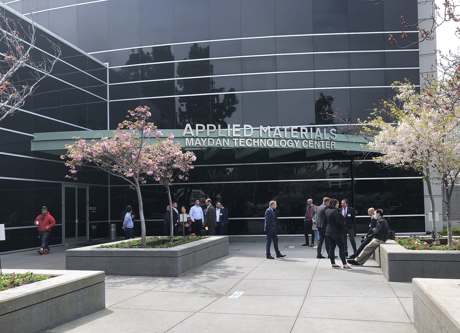
The Applied Materials EPIC Center — EPIC stands for Equipment and Process Innovation and Commercialization — was unveiled on October 12 in a company announcement that reads, in places, like an argument with the industry's own history. The facility, in Sunnyvale, California, represents a $5 billion capital investment. Applied describes it as the world's largest facility dedicated to collaborative semiconductor process technology and manufacturing equipment research and development: 600,000 square feet in total, nearly four acres of it cleanroom, built over more than six million construction hours. Leading chipmakers, systems companies, equipment partners and universities have committed to developing technology inside it.
To understand why that is a departure, consider how chips have been developed for forty years. Each manufacturer guarded its process recipes as crown-jewel secrets; equipment makers like Applied developed tools in their own labs, shipped them to customers, and iterated through a slow relay of trials behind fab walls. EPIC inverts the geometry. Instead of the relay, the participants work in the same cleanroom, on the same equipment generations, at the same time — trading a measure of secrecy for speed. Applied's chief executive, Gary Dickerson, framed the logic in the announcement: the scaling of AI infrastructure is driving chipmaking complexity to unprecedented levels, and the industry has to re-engineer how it collaborates if it wants development cycles to keep up.
Why a tools company is building a shared factory for ideas
Applied Materials is not a chipmaker. It sells the machines that make chips — deposition, etch, inspection and process-control systems that sit inside every advanced fab on earth, including the ones behind the output described in our TSMC record-revenue and 2nm ramp coverage. That position explains both the investment and its timing. When AI demand pulls chip designs toward new architectures — denser packaging, new materials, features measured in handfuls of atoms — the bottleneck increasingly appears before production, in the process-development stage where a design becomes a manufacturable recipe. A tools vendor that hosts that stage does not just sell equipment; it becomes part of the industry's research infrastructure, with early sight of where every major customer's roadmap is heading.
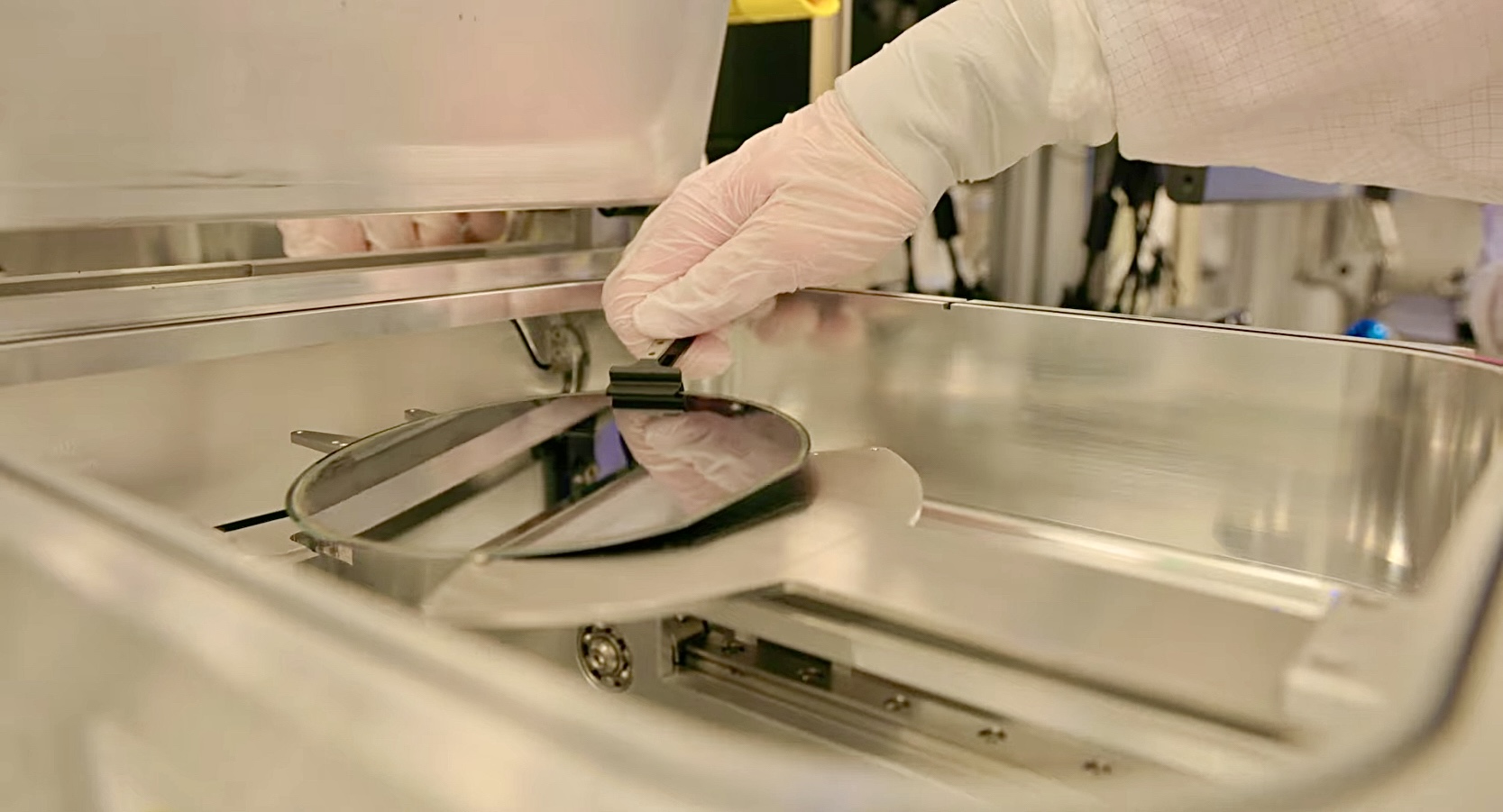
The scale figures deserve context. Five billion dollars is the kind of sum governments announce for national semiconductor programmes; it is a very large number for a single corporate R&D facility, even one built over years in Silicon Valley. Six hundred thousand square feet with roughly four acres of cleanroom puts EPIC in the size class of a working fab rather than a laboratory — which is precisely the point. Process development done at pilot scale, on production-class equipment, transfers to real fabs faster than work done on bench tools. Applied is buying down the industry's most expensive delay: the gap between a process that works in research and one that yields in volume.
Why this matters
Every era of the chip industry has had an organisational invention as important as its technical ones — the foundry model, the fabless model, the open instruction set. EPIC is a candidate for this era's. The technical problem it addresses is real: at the frontier, progress no longer comes from a single company optimising a single step. Transistors, materials, lithography, packaging and the software that designs them all interact, and the interactions are where yields — and therefore money — are lost. A shared facility where a chipmaker's process engineers, a systems company's architects and Applied's equipment scientists can run the same wafers through the same tools attacks the interaction problem directly. The commercial logic is just as clear, and it is the same logic driving the platform battles in our coverage of Microsoft's custom AI silicon push: in a supply-constrained AI build-out, whoever removes months from development time captures value that dwarfs the rent.
There is also a geographic argument embedded in the concrete. The United States has spent the past four years, through subsidy and export policy, trying to re-anchor advanced semiconductor capability onshore. Fabs have drawn the headlines, but a frontier process developed abroad cannot simply be photocopied into an American fab — the knowledge lives in people, recipes and tool configurations. A $5 billion collaborative process-R&D centre in Sunnyvale is the research end of that re-anchoring: it makes Silicon Valley a place where the next manufacturing generations are not just designed but worked out, physically, wafer by wafer. Whether universities' presence in the building produces the workforce pipeline to match is an open question, but the intent is unmistakable.
The awkward market reaction — and what it actually says
The stock market's first verdict was ungrateful. Applied's shares fell about 3.4% on the day, flagged in Barron's movers coverage, in the middle of a broader chip selloff — the same risk-off wave that ran through Asian markets in the KOSPI chip selloff this week. It would be a mistake to read the fall as a judgment on EPIC itself. The selloff's logic, as traders described it, was about the aggregate: investors are beginning to interrogate the returns on the AI industry's enormous capital spending even as the spending itself keeps accelerating. Applied is exposed to that question twice — its own $5 billion is now part of the capex mountain, and its revenue depends on customers continuing to climb it. A tools company announcing a record R&D facility on a day when the market is asking whether there is too much investment is a coincidence of timing, but a revealing one: the industry is now large enough that its investment announcements move the very anxiety they are meant to answer.
Who benefits, who loses, and what the critics say
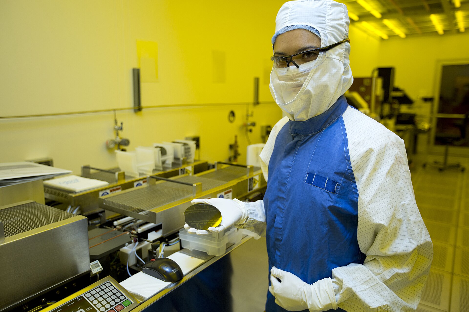
Applied benefits if EPIC becomes what it intends: the default room where next-generation processes are proven, which would pull equipment evaluations, and eventually orders, toward Applied's tools by familiarity as much as by merit. Chipmakers benefit from faster process development without each building a $5 billion facility of their own — particularly second-tier manufacturers for whom a shared centre is the only affordable route to frontier process work. Universities gain access to production-class cleanroom space their own budgets could never buy, and students gain a direct path into the industry's scarcest skill set.
The risks are symmetric. Collaboration among competitors has a hard boundary at the point where a participant's process becomes its advantage; critics reasonably ask how much of the truly valuable work companies will actually bring into a shared building, rather than keeping in-house and sending EPIC the safer, pre-competitive projects. If that is what happens, EPIC still functions — pre-competitive process research is genuinely valuable — but as an industry utility rather than the invention engine of the announcement's framing. There is also an antitrust-adjacent sensitivity whenever direct competitors share facilities and roadmaps; the centre's governance will need to be visibly careful. And the sceptics of the AI capex cycle make the simplest point of all: a $5 billion facility is a fixed bet on demand a decade out, placed at the moment investors are loudest in asking whether that demand will pay for itself.
What happens next
The milestones that matter are operational, not rhetorical: which named chipmakers and systems companies actually install teams and run development programmes inside EPIC, what process generations the centre targets first, and whether any production process can be publicly traced back to work done there. Expect the first claims within a couple of equipment cycles — in this industry, the honest unit of time. The other watch-point is imitation. If EPIC's model works, rival equipment makers will face pressure to offer their own collaborative facilities, and the geography of chip R&D will tilt further toward shared mega-labs. Applied has spent $5 billion on a proposition: that in the AI era, the fastest way to invent a chip process is together. The industry's most secretive business is about to test it in four acres of cleanroom.
Sources
- Applied Materials — EPIC Center announcement, GlobeNewswire, October 12, 2026: globenewswire.com and appliedmaterials.com
- Barron's — market movers coverage of Applied Materials shares amid the October 13 chip selloff, 2026.
- Signal Post News — related coverage linked in the text above.